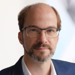
Rolf Aschenbrenner received a B.Sc. in mechanical engineering in 1986 and an M.Sc. in physics in 1991 from the University of Giessen. In 1994, he joined the Fraunhofer Institute for Reliability and Micro-integration in Berlin (IZM), where he is presently head of the department for chip interconnection technologies, and deputy director of the institute. Rolf Aschenbrenner’s research work spans from manufacturing process fundamentals to applied manufacturing problems. He has made substantial research contributions in thin and flexible electronic assemblies, end the development and analysis of innovative process technologies for all aspects of system level packaging. He served on various committees, and in 2013 he received the IEEE CPMT David Feldman Award.
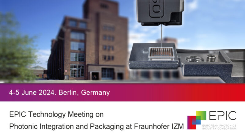

EPIC Meeting on Integrated Photonics at Fraunhofer IZM, a groundbreaking event that brings together industry leaders, experts in photonics, and end-users from around the globe in the dynamic realm of integrated photonics. Hosted by the prestigious Fraunhofer Institute for Reliability and Microintegration (IZM), this meeting aims to foster collaborative discussions and explore the frontiers of integrated photonics technology and scalable packaging of photonic chips. As the demand for faster, smaller, and more efficient electronic devices continues to surge, integrated photonics has emerged as a transformative technology. It offers a myriad of opportunities to revolutionize various sectors, including telecommunications, data centers, healthcare, and sensing applications. Fraunhofer IZM, renowned for its pioneering research in microsystems and packaging technology, is at the forefront of advancing integrated photonics, enabling innovative solutions with unparalleled performance and reliability. The EPIC Meeting serves as a nexus where industry pioneers, entrepreneurs, investors, researchers, and decision-makers can converge to exchange knowledge, share experiences, and collaborate on the future prospects of integrated photonics. With an emphasis on scalable packaging of photonic chips, participants will delve into cutting-edge advancements in chip-scale integration, heterogeneous integration, advanced packaging techniques, and novel manufacturing processes.
All paticipants biographies, photos and company descriptions are available HERE.

Rolf Aschenbrenner received a B.Sc. in mechanical engineering in 1986 and an M.Sc. in physics in 1991 from the University of Giessen. In 1994, he joined the Fraunhofer Institute for Reliability and Micro-integration in Berlin (IZM), where he is presently head of the department for chip interconnection technologies, and deputy director of the institute. Rolf Aschenbrenner’s research work spans from manufacturing process fundamentals to applied manufacturing problems. He has made substantial research contributions in thin and flexible electronic assemblies, end the development and analysis of innovative process technologies for all aspects of system level packaging. He served on various committees, and in 2013 he received the IEEE CPMT David Feldman Award.
Henning Schröder received his M.Sc. degree in applied physics from the University of Magdeburg, Germany in 1994 and his Ph.D. degree at the Technical University of Berlin in 2000. Currently, he is with Fraunhofer IZM, heading the Optical Interconnection Technologies Group. His main fields are R&D of photonic packaging and optical interconnection technologies for printed circuit boards and photonic modules. The research focus lies on the design, fabrication and performance enhancement of optical glass waveguides and micro optics for PCB and optical sensors, their characterization, and on reliable micro-optical assembling and packaging technologies for photonic modules, including optical fiber attachment. He holds a lot of patents in photonic packaging technologies. Henning is member of the German Physical Society, German Society of Applied Optics, and European Optical Society.

Elvis Wan received his Professional Doctorate in Engineering degree from Eindhoven University of Technology, with strong focus on process development and optimization. Before he relocated to the Netherlands, he finished his Master’s Degree in Mechanical Engineering from University of Hong Kong. He joined PhotonFirst in 2016. Specializing in photonic chip packaging, Elwis excels in process setup, optimization, and project management. He leads key work packages in the PIXAPP project, aimed at standardizing photonic chip packaging technologies. Elwis is adept at designing demonstrator packages for fiber sensing applications and evaluating external packaging requests. His expertise lies in bringing together equipment and machinery, optimizing production processes, and managing projects effectively.
Rudolf Heer leads the Electronic Sensors division at Silicon Austria Lab GmbH (SAL) in Graz, Austria. He is an expert in the design and fabrication of readout electronics and signal processing units for nano-scale devices and sensors. He graduated in electrical engineering from the Vienna University of Technology in 1996. During his diploma thesis, he deepened his knowledge of laser physics. His doctoral studies focused on low-temperature semiconductor physics. He also served as a lecturer. After completing his doctorate in 2000, he joined EPCOS OHG in Munich, where he was responsible for integrating radiofrequency front-end modules for cell phones. In 2002, he moved to Applied International Informatics AG in Vienna, focusing on sizing and performance tuning of SAP/R3 systems. From 2004 until 2019, he led the nano-components research group at the Austrian Institute of Technology, concentrating his research on biosensors and microfluidics for molecular diagnostics. Since 2019, Rudolf Heer has been the head of the research unit and, since 2021, a principal scientist at SAL.
Hanno Scheife is a highly skilled physicist with a focus on optical systems and laser physics. He earned his Diploma in Physics from the University of Hamburg in 1997, followed by his Doctorate in Natural Sciences in Physics from the same institution in 2001. His career spans over 17 years at TESAT, a leading company in the aerospace industry. Hanno has played pivotal roles within TESAT, starting as a System Engineer and progressing to leadership positions such as Team Leader for Optical Modules & Systems and, currently, as the Team Leader for Optical Unit Assembly, Integration & Test. Before joining TESAT, he worked as a research assistant at the Institute for Laser Physics at the University of Hamburg.

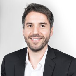
Moritz Seyfried received a Master’s degree from the Heriot-Watt University in Edinburgh as well as a diploma degree from Karlsruhe Institute of Technology in physics. Both works took place in the field of organic and anorganic semiconductor optics. His PhD work was carried out in the framework of the DFG project "Use of coupling effects in II-VI based monolithic microcavities for low threshold laser” at the University of Bremen. After finishing his PhD and a short PostDoc stay he joined the Research & Development team at ficonTEC in 2012 where he is setting up new R&D projects and is implementing new technologies into existing alignment and bonding machines.
Robert Kirchner develops multi-material 3D printing since 2018. He has an engineering degree from Technische Universität Dresden and has 10+ years of experience in 3D micro-nano-fabrication. Robert drives the vision, the strategic development, and supports the system design. He has a background in electrical engineering and received his PhD in polymer microsystems fabrication in 2011. During his PhD, and especially afterwards in his professional positions, such as at the Fraunhofer Institute for Photonic Microsystems (IPMS) and the Paul Scherrer Institute, he did intensive research in the fields of nanoimprint lithography, grayscale lithography, and 3D printing using 2-photon absorption-based laser writing.
Jean-Luc Polleux is cofounder and CTO of ICON Photonics. Professor on leave from the University Gustave Eiffel – ESIEE Paris and researcher at CNRS-ESYCOM lab from 2001 to 2022, he received the PhD degree from the Cnam in 2001. His research involved photonics, microwaves and microtechnology with special emphasis on Silicon-based integration, high-speed photonic interconnects, microwave phototransistors (SiGe/Si and InGaAs/InP) and VCSELs. He published over 100 scientific communications and journal paper. In 2018, he cofounded ICON Photonics as a spin-off of his research activities at ESIEE Paris and ESYCOM. He is a member of the advisory board of the Hub Optics/Photonics - Systematic cluster.
Jörg Smolenski graduated from RWTH Aachen and Fraunhofer ILT, holds a Master Degree in Mechanical Engineering, and has an international background spanning more than 20 years in industrial laser technology. He started as international sales manager at Lumibird in France (formerly Quantel), joined their US subsidiary to transfer product know-how, and then developed sales at High Q Laser in Austria. After 12 years with TRUMPF, he has experience in key account management, business development, laser technology, international sales and industrial laser applications including welding, marking and micromachining. Jörg joined Nanoscribe in May 2019 as Business Development Manager. In this position, he focuses on mastering and replication technologies as well as integrated photonics.
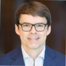
David de Felipe Mesquida has been contributing his expertise at Fraunhofer HHI since 2011. He holds a Doctor of Engineering in Photonics Engineering from the Technical University of Berlin (2019), a Master of Engineering in Telecommunications from the Polytechnic University of Valencia (2010), and a Bachelor of Engineering in Telecommunications from the University of the Balearic Islands (2007). David has progressively advanced at Fraunhofer HHI, previously serving as a Project Manager and Research Associate, and now oversees key projects in the field of photonics.
Joni Mellin is the Product Marketing Manager at X-Fab. Previously he served at ams OSRAM (2014-2021), where he held Engineering director and other positions in the Full-Service Foundry division. Prior to that, he served at Microsoft (2014), Nokia (2008-2014), Micro Analog Systems (1999 – 2008) and Helsinki University of Technology (1997-1999). He received his Licentiate of Science (Tech) (2012) and Master of Science (Tech) (1999) degrees in semiconductor technology from the Aalto University and a dual GEMBA degree from WU Vienna and University of Minnesota in 2019.
Thorsten Mayer joined Vanguard in 2020 and served as Chief Operating Officer (COO) for one year. Prior to joining Vanguard Automation, Thorsten has held several regional and global leadership positions at National Instruments (NI) in sales, strategic marketing and operations. Amongst his roles at NI he served as Managing Director for East-Central Europe quadrupling revenues and profits over seven years and led high-impact transformational projects at the global level as Chief of Staff and Global Head of Alliance Sales & Strategic Partnerships. He has lived and worked in four countries. Thus, he offers U.S. Corporate, European and Asian experience and a strong international background to business development and geographical expansion. Thorsten has also been contributing through his voluntary work at SWAN Impact Network, both as investor and advisor, to startups with measurable social or environmental impact.

Niels Jansen is responsible for the Engineering department at Etteplan Engineering Solutions in the Netherlands, including mechanical, electrical, software and process engineering. In his role, he is also responsible for the development of the machine platform and manufacturing production solutions, as well as the technology roadmap. Niels is member of the Management Team (MT) of Etteplan NL. Niels received his Master’s degree in Systems and Control from the Eindhoven University of Technology with the classification with great appreciation. Since then, he worked for several companies in the industrial automation in the Netherlands, where he gained positions as group leader and manager for engineering teams, responsible for the development and implementation of industrial automation solutions.
Thomas Achleitner is a Business Development Manager at EV Group, concentrating on Micro and Nanoimprinting for diverse applications, such as nanophotonic elements and wafer level optics. Thomas holds a degree in Innovation and Product Management from University of Applied Sciences Upper Austria. He has accrued six years of experience as a Senior Process Engineer in Nano Imprinting Lithography, specifically focusing on diffractive optical elements for Augmented Reality and Virtual Reality devices.
Steffen Diez has 2 decades of experience in the field of Laser Lithography. He joined Heidelberg Instruments in 2000 to lead the conversion software group. From 2005 to 2010 he managed several projects for Direct Write PCB Exposure Systems resulting in the introduction of new SLM based Light Engines into Heidelberg Instrument’s product portfolio for the first time. During a one year stay in Japan, Steffen was responsible for Technical Sales and Business Development in Asia. In 2012, under Steffen’s leadership as Product Manager, Heidelberg Instruments introduced the Maskless Aligner: The introduction of the new DMD based Direct Write Lithography tool was the most successful product launch in the company’s history. From 2012 to 2019, In addition to his position as Product Manager, Steffen also headed the Process and Application Lab in Heidelberg. He was a member of the Technical Board for several years before becoming Chief Sales Officer in 2017. Since 2019, he is the Chief Operating Officer of the company. His exceptional experience in R&D, Marketing and Sales helps to support worldwide sales and expand HIMT’s Business Development activities in the respective markets. Steffen received his Diploma in Electrical Engineering from the Karlsruhe University in 1999.

Daniel Lieske is an experienced process engineer specializing in electronic engineering. He earned his diploma in electrical engineering from the Brandenburg University of Technology Cottbus-Senftenberg in 2005. Daniel's career spans nearly two decades in the engineering field, with significant roles in various companies. Currently, Daniel serves as a Process Engineer at AEMtec, where he has worked for over 13 years, starting as a Development Engineer. Prior to AEMtec, he gained valuable experience in the same role at Freudenberg NOK Mechatronics and at Qimonda.

Sebastian Haag received his diploma in Electrical Engineering at the RWTH Aachen University in the year 2010. Afterwards, he worked as a scientist and group manager at the Fraunhofer Institute for Production Technology IPT in Aachen in the field of automation and optical packaging until 2016. During his scientific carrier, he focused on the development of software toolchains for modelling complex optical alignment, packaging tasks and robotic control.
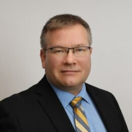
Hektor Meier received his MSc in Electrical Engineering from the Swiss Federal Institute of Technology (ETH) in 2006. That same year, he joined the computational optoelectronics group at the Integrated System Laboratory at ETH Zurich as a research assistant, focusing on the numerical simulation of non-equilibrium carrier transport. In 2011, he earned his PhD degree and subsequently joined the product development team at Enablence Switzerland, where he worked on developing high and ultra-high speed InGaAs PIN and avalanche photodiodes. Currently, Hektor is the Head of Product Development at Albis Optoelectronics, overseeing the ongoing development and expansion of the company's photodiode portfolio.
Eric Mounier is Fellow Analyst at Yole Group (Yole), with more than 25+ years’ experience within the semiconductor industry. He provides daily in-depth insights into current and future semiconductor trends, markets and innovative technologies (such as Quantum computing, Si photonics, new sensing technologies, new type of sensors ...). Based on relevant methodological expertise and a strong technological background, he works closely with all the teams at Yole to point out disruptive technologies and analyze and present business opportunities through technology & market reports and custom consulting projects. With numerous internal workshops on technologies, methodologies, best practices and more, Yole’s Fellow Analyst ensures the training of Yole’s Technology & Market Analysts. In this position, he has spoken in numerous international conferences, presenting his vision of the semiconductor industry and latest technical innovations. He has also authored or co-authored more than 100 papers as well as more than 120 Yole’s technology & market reports. Previously, Eric held R&D and Marketing positions at CEA Leti (France). Eric has a PhD. in Semiconductor Engineering and a degree in Optoelectronics from the National Polytechnic Institute of Grenoble (France).
Lee Jae-Wung majored in Material Science and Engineering and got a Ph.D. degree at Seoul National University in Aug 2008. Now he has been researched Si photonics and MEMS field as research scientist at VTT in Finland. His Ph.D. research was focused on Fabrication and evaluation of piezoelectric materials. He fabricated piezo-and ferroelectric films with many kinds of deposition processes; sputtering, e-beam, sol-gel coating. And optimized processes for increasing their property. After PhD, he worked as a research associate in Esashi lab; Tohoku University in Japan. His works were development and fabrication of functional materials such as piezoelectric materials and metallic glass materials for MEMS device. He also carried out MEMS device design and simulation for sensors, actuators and so on as well as their fabrication for 3 years. After research at Tohoku University, he worked for A*STAR IME in Singapore for 8 years. His work was process design, development and fabrication of the MEMS devices and their wafer level packaging ex. pMUT devices using AlN and PZT for fingerprint and medical device, micro-switches with thin film packaging, gas sensors, Al-Ge bonding for gyroscope, accelerometer and magnetometer. He has joined VTT and worked for 6 years from 2018. At VTT, his work is developing hybrid integration/3D packaging of Si photonics/MEMS/IPDs. He is also developing deep TSV as well as solder development for flip-chip bonding. Currently he is focusing on precise optical alignment for PICs with III-V components for Si photonics’ applications.
Liron Gantz is currently the manager of Nvidia's Electro-optics group, which spearheads advancements in silicon photonics technology for Co-Packaged products. His group also explores innovative ways to utilize AI and GPU acceleration to enhance silicon photonic design, pushing the boundaries of high-speed Datacom communication. Graduating in 2017 with PhD in Electrical Engineering from the Technion, Israel Institute of Technology, he swiftly transitioned into leadership roles, focusing on design, characterization, and modelling of silicon photonic technology. With a strong background in Quantum Mechanics, Nanotechnology, and Optics, Liron Gantz has authored impactful papers in prestigious journals like Science and Physical Review Letters, showcasing his expertise and contributions to the semiconductor industry.
Jeroen Duis received his bachelor’s degree from the Technical University of Rijswijk in 2001. After his study he worked 16 years within TE Connectivity. Within the Fiber Optic Business Unit and corporate technology team he held several positions in engineering, research, technology scouting and management. During this time, he gained a broad experience in: laser processing of glass fibers, WDM multiplexing, low loss optical interconnects, next generation photonic chip packaging for applications in mobile phones, automotive and high speed computing applications. In March 2017 he accepted a position at SMART Photonics, a scale up in Indium Phosphide wafer manufacturing where he was responsible for the business development. November 2018, Jeroen accepted a position as Chief Commercial Officer at PHIX photonics assembly where he is responsible for the commercial activities and the strategic direction for the hybrid packaging. He is the author and co-author of several publications and holds 15 patent applications in the field of optical interconnection technology.
Joan Felip is the Automation Manager at VLC Photonics, a position he has held since September 2016. He has over 7 years of experience in this role, contributing to the company's success in the field of photonics. Joan holds a Master's degree in Telecommunications Engineering from the Universitat Politècnica de València (UPV), which he completed in 2016, following his Bachelor's degree in Engineering of Telecommunication Technologies and Services, also from UPV, which he obtained in 2014.
Sophie Lange has been a part of EXFO since 2021, specializing in PIC testing solutions. Previously, she was a researcher at Microsoft Research in Cambridge (2018-2021), focusing on ultra-fast tunable lasers for optically switched data center architectures. Sophie earned a PhD from TU Berlin, developing high-speed InP transmitter PICs at Fraunhofer HHI. She also holds an Erasmus Mundus Master’s degree, graduated in 2012 from Aston University in Birmingham and Scuola Superiore Sant’-Anna Pisa, with her master’s thesis completed at Osaka University. Her blend of industry and research experience make her a valuable asset in the photonics field.
Björn Globisch is head of the R&D and frontend department of TOPTICA EAGLEYARD. TOPTICA EAGLEYARD develops wavelength stabilized, high power laser diode modules for the wavelength range between 630 nm and 1120 nm. As head of the R&D and frontend department he is responsible for the development of innovative packaging solutions and laser chip designs. Before he joined TOPTICA EAGLEYARD in 2023, Björn was assistant professor for terahertz sensing at Technical University Berlin, Germany, and head of the terahertz sensorsystems group at Fraunhofer institute for telecommunications, Heinrich Hertz Institute (HHI) in Berlin, Germany. Björn holds a PhD in physics from Philipps-University Marburg, Germany.
- Abdul Rahim , Eco System Manager at PhotonDelta
- Aivars Vembris , Senior Researcher at Institute of Solid State Physics
- Alex Borodkin , Scientist, Optical Integration Research Group at Innolume
- Alexander Bachmann , Senior Director R&D Technology at TOPTICA Photonics
- Aljoscha Shu , Founder / CEO at Photonics Foundry
- Andreas Pichler , Regional Sales Manager Europe at EV Group (EVG)
- Arkady Shipulin, Consulting at Star Photonics
- Arslan Sajid Raja , Development PIC Engineer at Menlo Systems
- Arturs Bundulis , Leading Researcher at Institute of Solid State Physics
- Axel Schönau , Deputy Head of Group at Fraunhofer Heinrich Hertz Institute
- Bart Oude Lohuis , System Architect at IMS
- Björn Globisch , Head of R&D / Frontend at TOPTICA Eagleyard
- Bruce Valentine , Global Managing Director at OpTek Systems
- Chris Lewins , Quantum Processor Engineering Team Lead at Oxford Ionics
- Daniel Lieske , Senior Expert Advanced Packaging at AEMtec
- David de Felipe Mesquida , Senior Project Manager at Fraunhofer HHI
- Elvis Wan , Senior Industrialisation Engineer at PhotonFirst
- Eric Mounier , Chief Analyst at Yole Group
- Fabian Mohn , Staff Engineer at Lumiphase
- Frank Laas, Engineer Field Sales DACH at PI
- Gerd-Albert Hoffmann , Head of Optics Integration Work Group at Laser Zentrum
- Gernot Wolkenstein , Business Development Manager at Tresky
- Gijs Brienen , Sales/Marketing at Mintres
- Gunnar Boettger , Industrial Relations Manager in Group OIT at Fraunhofer IZM
- Hanno Scheife , Team Leader at TESAT
- Hardy Kellermann, Head of Development and Deputy Head of Application at ASMPT AMICRA
- Hektor Meier , Head of Product Development at Albis Optoelectronics
- Hendrick Thiem , Development Engineer at TOPTICA Eagleyard
- Henning Schröder , Group Manager at Fraunhofer IZM
- Hermann Oppermann , Group Manager Fine Pitch Assembly and Interconnects FPAI at Fraunhofer IZM
- Hidenori Yoshioka, Manager at DNP Europa
- Inna Krasnokutska , Lead Photonic Engineer at Xanadu Quantum Technologies
- Isabelle Faggianelli , EU Lead Scout at PERCIPIO ROBOTICS
- Ivan-Lazar Bundalo , CTO at InSpek SaS
- Jae-Wung Lee , Reseach Scientist at VTT
- Jan-Jurien de Rijck , Business Development at PhotonFirst Technologies
- Jean-Luc Polleux , Co-Founder and CTO at ICON Photonics
- Jean-Yves Bécel , Export Account Manager at ISP System
- Jeroen Duis , Chief Commercial Officer at PHIX
- Jesper Jensen , CTO, Founder at Bifrost Communications
- Joan Felip , Automation Manager at VLC Photonics
- Johana Bernasconi , Lead Engineer at Enlightra
- Joni Mellin , Product Marketing Manager Photonics at X-FAB
- Joost de Laat , Policy Advisor International Affairs at Provincie Noord-Brabant
- Jörg Smolenski , Business Development Manager at Nanoscribe
- Krzysztof Anders , Integrated Photonics Team Manager at VIGO Photonics
- Krzysztof Machałowski, Assembly Technology and Optical Engineer at Vigo Photonics
- Kun Li , Facilities Director at King Abdullah University of Science and Technology
- Laura Gemini , Deputy Head Laser Processing Dpt. at ALPhANOV
- Laura Horan , Staff Engineer - Product Management Lead at Vanguard Automation
- Liam Moroney , Business Development Manager at Alter Technology
- Liron Gantz , Manager of the Electro-Optics Group at NVIDIA
- Logen Dilli , Account Manager at IMS
- Maria Russew , Unit Manager Hybrid Polymers at micro resist technology
- Martin Schell , Executive Director at Fraunhofer HHI
- Matthäus Banach , CTO at Finetech
- Maurine Malak , Senior Packaging Engineer at Swiss-PIC
- Melanie Macioce , R&D Photonics Engineer at PERCIPIO Robotics
- Michael Scholles , Business Development Manager at Fraunhofer IPMS
- Mikko Karppinen , Research Team Leader – Photonics and RF Integration at VTT
- Moritz Seyfried , Director Research & Development at ficonTEC
- Niels Jansen , Manager Engineering at Etteplan
- Nikola Prtljaga , Senior Photonics Engineer at Bay Photonics
- Patrick Wu , Director of Nano Photonics at Huawei
- Peter Visser , Project Manager at PhotonDelta
- Pierre Wahl , Global Sales Manager at Luceda Photonics
- Pooya Saketi , CEO/Founding Director at Precisement
- Rafał Ciechański , Microelectronics Assembly and Packaging Engineer at Vigo Photonics
- Robert Kirchner , CEO & Co-Founder at HETEROMERGE
- Rolf Aschenbrenner , Institute Deputy Director IZM at Fraunhofer IZM
- Ronald Dekker , CTO at LioniX International
- Rudolf Heer , Head of Research Unit Electronic Sensors (ELS) at Silicon Austria Labs
- Ryszard Piramidowicz , PIC Programme Director at VIGO System
- Samuel Mottier , Senior Product Manager at ETEL
- Sebastian Haag , CEO at AIXEMTEC
- Shabbir Bashar, Head of Manufacturing Operations at Salience Labs
- Simon Kibben , CTO at Photonics Foundry
- Simon Schwinger , CEO at Jenaer Antriebstechnik
- Simon Wichmann , Field Sales at Physik Instrumente (PI)
- Sophie Lange , Business Development Engineer at EXFO
- Stephan Mannshardt , Product Manager at TOPTICA Eagleyard
- Steffen Diez , Chief Operations Officer at Heidelberg Instruments
- Thomas Achleitner , Business Development Manager at EV Group (EVG)
- Thorsten Mayer , CEO at Vanguard Automation
- Tolga Tekin , Group Manager Photonic & Plasmonic Systems PPS at Fraunhofer IZM
- Ton Offermans , Project Manager at CSEM
- Trevor Demille , Head of Quantum Components and Laboratories at QuiX
- Wilfried Noell , Chief Scientist at Focuslight
- William Fegadolli , Director of Optical Technologies at Nokia
- Xin Gong , Senior Sales Manager and Technical Business Development at Engionic Femto Gratings
- Yvonne Voedisch , Head of Application at Jenaer Antriebstechnik
- Zewang You , Team Lead Material and Core Process at Vanguard Automation
- Zheng Han , Strategic Research Manager at Huawei


Market Reports
Upcoming Events


Related
Past Events