22 June 2026
/ 15:00
- 17:00
CEST
EPIC Online Technology Meeting on Laser Processes for the Semiconductor Industry
Online Event
Laser processes have become essential tools in the semiconductor industry, offering high precision, minimal thermal impact, and flexibility for a wide range of fabrication steps. Ultrafast and short-pulse lasers are increasingly used for applications such as wafer dicing, micro-drilling, patterning, marking, and material ablation, enabling damage-free processing of delicate and multilayered semiconductor materials. Laser annealing and laser lift-off techniques are also widely adopted for enhancing material properties, enabling layer separation, or improving carrier mobility in advanced semiconductor structures. With the growing demand for smaller feature sizes, advanced packaging, and heterogeneous integration, laser-based processes provide the necessary accuracy and throughput while supporting non-contact, contamination-free operations. Innovations in beam shaping, pulse-on-demand technology, and process monitoring are further expanding the capabilities of lasers in semiconductor manufacturing, supporting next-generation chip production and enabling more efficient and scalable device fabrication.
We invite the whole supply chain to discuss about the latest developments on lasers for the semiconductor industry and to understand the challenges and needs to be solved in the future.
Agenda
Speakers

Natan Kaplan, M.Sc. in Applied Physics from TAU, is the CTO of Holo/Or with over 12 years of experience specializing in diffractive components for high precision laser systems.
CTO
at HoloOr

After postdocs in France and Germany, she co-founded RayVen Lasers GmbH in 2025 and she serves as CEO.
CEO & Co-Founder
at RayVen

Maurice Clair studied Mechanical Engineering at the University of Technology Chemnitz (Germany). He joined 3D-Micromac in 2005 as a development engineer and is now team leader of the technology and innovation management department.
Team Leader Technology & Innovation Management
at 3D Micromac

CEO
at Femtum

Michał Ćwikła is a laser microprocessing specialist at the Fluence Technology Application Laboratory, joining the company in 2025. He specializes in developing laser processing techniques, designing optical systems, and conducting internal R&D projects. He completed his PhD at the Faculty of Mechanical Engineering at Wrocław University of Science and Technology, focusing on liquid-assisted laser processing. He is the author of eight publications in the fields of laser processing and the design of optical systems for process monitoring.
Laser Microprocessing Engineer
at Fluence Technology

Robert Kirchner (Co-Founder & CEO) develops multi-material 3D printing since 2018. He has an engineering degree from Technische Universität Dresden and has 10+ years of experience in 3D micro-nano-fabrication. Robert drives the vision, the strategic development, and supports the system design. He has a background in electrical engineering and received his PhD in polymer microsystems fabrication in 2011. During his PhD, and especially afterwards in his professional positions, such as at the Fraunhofer Institute for Photonic Microsystems (IPMS) and the Paul Scherrer Institute, he did intensive research in the fields of nanoimprint lithography, grayscale lithography, and 3D printing using 2-photon absorption-based laser writing.
CEO & Co-Founder
at Heteromerge

VP Sales and Marketing
at Luxinar
Attendees
- Abel Gil Villalba , Head of Developement and Industrialisation at DM SURFACES
- Adam Hegedues, Researcher at HiLASE
- Ahmad ODEH , Senior Scientist-Laser R&D Project Leader at The Swatch Group
- Aivaras Urniezius , Strategic Sales Manager at Light Conversion
- Alain Chardon , Director at ArzhOptics
- Alan Bulian , Technical Business Development & NPI Manager at StarTech Trieste
- Alejandro Madrid Sanchez , Researcher at Vrije Universiteit Brussel
- Alessandro Tonon, Laser Process Engineer at Kirana
- Alessio Bruttomesso, Sales Manager at Optoprim
- Alexander Telle , CEO at ACM Coatings
- Amir Hossein Ghadimi , CEO at Lightium
- Andrea Lucca , technical sales at bright solutions
- Andrea Teuber, Technical Sales at Mountain Photonics
- Andreas Brand , Business Developer Laser Technologies at Fraunhofer ISE
- Andreas Gaab, Head of Technical Competence Center at Raylase
- Andreas Rudolf , CEO at PT Photonic Tools
- Andrew Zielecki, Laser Applications Engineer at Photon Automation
- Anne Maiwald , Marketing Manager at Active Fiber Systems
- Antoine Courjaud , Strategic Business Development at Amplitude Laser
- Antonio Cabas Vidani , Product Manager at Fluxim
- Antonio Raspa , Laser & LiDAR at Luxinar
- Antti Salminen , professor at University of Turku
- Arindom Phukan , Post Doctoral Scientist at HiLASE
- Armi Fernandez , Process Engineer at Texas Instruments
- Arnas Žemaitis , Head of Sales at Femtika
- Artur Piscalov , Product manager at STANDA
- Arturo Elias Llumbet , Market Analyst at Tematys
- Athul Som, Optical Engineer at Lidrotec
- Attila Werner , Sales at Primes
- Ayalon Alex , Senior Director, R&D and Innovation at Elbit Systems
- Aymen Chargui , International Business Developer at AUREA Technology
- Aymeric LECOT , International Sales Manager and Product Marketing Lead at Teem Photonics
- Benjamin Bernard , Team Lead Application at DISCO HI-TEC Europe
- Benoit Beaudou, Application Engineer at GLOphotonics
- Cedrik Coia , Chief Scientist at AEPONYX
- Celia Millon , CEO & co-founder at RayVen
- Chris Randon , Business Development Manager at Optek Systems
- Christopher Rowan , Managing Director at Arscientia
- Christos Markos , Associate Professor at Technical University of Denmark (DTU)
- Clémentine Maurier, Product Manager at Cailabs
- Csilla Timar-Fulep , Applications Engineering, Senior Supervisor - Optics Photonics Workflow at Ansys UK
- Dauksa Arunas , Sales at Femtika
- David Bruneel , Group research Coordinator at LASEA
- David Ettel , CEO at NANOTECHNA
- David Horain , Director at BLOOM Lasers
- Degenhart Hochfilzer, New Business Development Manager at Schott
- Deividas Andriukaitis , Senior Industrial Laser Sales Manager at Ekspla
- Diego ORMAECHEA , Technical Sales Engineer at imagine Optic
- Domas Baliukonis , Product manager at Light conversion
- Dominique Bonnisseau , CEO at Photonikbiz
- Doyinsola Sonoiki, Postdoctoral researcher at Technical University of Denmark
- Dragan Velkov , Principal Applications Engineer at Edmund Optics
- Elena Sokolova , optical engineer/designer at RiverD International
- Emma Modrate, Sales at PowerPhotonic
- Erwin Moench, Development Engineer at Chips 4 light
- Eugen Bärwald , Business Development Europe at MPS Micro Precision Systems
- Evangelos Skoulas , CTO at Biomimetic
- Evelien Evelien, Associate at PhotonVentures
- Fabrizio Garnero , Editorial Director at DBinformation
- Federico Fabrizi , Innovation & Business Development Engineer at Lithium Lasers
- Felix Malcher, Product manager at Scanlab
- Florian Hermann, Ingenieur at Precitec
- Florian Tauser , Senior Director R&D at TOPTICA Photonics
- Francesco Antolini , Researcher at ENEA
- Fredrik Johansson, R&D Engineer at Coherent
- Gediminas Raciukaitis , Head of Department of Laser Technologies at FTMC
- Geoff Shannon , Principal at Laser Markets
- Giorgio Cazzaniga , Product Management Senior Director at JABIL
- Gregory Flinn, Marketing Development at ficonTEC Service
- Guillaume Szymczak , Sales manager Apac at Lasea
- Haider Al-Juboori , R&D at South East Technological University SETU
- Harvey Washbrook , Sales Manager at Laser Components
- Herve Besaucele , CTO at GenF
- Ioan Notingher , Professor at University of Nottingham
- Iossif Elenkov , R&D Engeneering at EXCELITAS
- Jana Lambrecht , Business Development Manager at Excelitas
- Jaroslaw Sperling , Business Development at Menlo Systems
- Jean-Francois Cormier , Scientific Advisor at INO
- Jean-Francois Poisson , Industrial Sales FR/CH/BE at Light Conversion
- Jens Biesenbach , GM at BWT Laser Europe
- Jens Schwerdtner , Project Engineer Technical Sales at Photonic Tools
- joe delfino , Founder at Salescycle
- Joerg Nowack , Senior Strategist, EMEA Corporate Strategy Office at Hitachi High-Tech
- John Golub , Founder at Groove Laser
- Jonas Wiedenmann , Technical Application Manager at Heidelberg Instruments
- Jonathan Wood , R&D Engineer at Synova
- Jürgen Stollhof , CSO - Director Sales & Marketing at Sill Optics Group
- Justinas Pupeikis , CEO at K2 Photonics
- Karina Kovalenko , Marketing and Communications Manager at VoxelSensors
- Kasun Dissanayake , Researcher at Delft University of Technology
- Katarzyna Szykula-Meurs, CSO at Coher Sense
- Katy Voisey, Associate Professor at The University of Nottingham
- Kenneth Kaufmann , Business Development at Photonics Management
- Kevin Kim, R&D Engineer at DM Surfaces
- Kimon Moratis , Market Intelligence Lead at Tematys
- Koji Tatsumi , Manager at Mitsubishi Materials Tools Europe
- Krzysztof Anders , Integrated Photonics Team Manager at VIGO Photonics
- Léo Jourdy, Optical Design at Latecoere
- Lida Shamsafar , Researcher at university of stuttgart
- Louis-Rafael Robichaud , CEO at Femtum
- Lu Lu , Engineer at Xfab
- Luigi Calabrese , CEO at Yalosys
- Luz Ruiz , General Manager at Pro-Lite Technology Iberia
- Lyes Kadi, Development Engineer at HUBER+SUHNER
- Manoj Kumar , Sales Engineer Europe at ficonTEC Service
- Mans Torsten , BD Semi at Trumpf Laser
- Marek Mach , Project manager for metrology and Partner for Semicon at asphericon
- Marijke Keters , Head of the semiconductor portfolio at Sensinnovat
- Mark Thompson , CEO at Lumenox
- Mark Weingarten , VP BusDev at Laserline
- Martin Eckstein , CTO at Lumics
- Martin Paster , VP Sales & Marketing at Luxinar
- Martynas Dagys , VP Business Development at Workshop of Photonics
- Mathieu Semenou , CCO at Femto Easy
- Matteo Verdi, R&D at Kirana
- Matthäus Banach , CTO at Finetech
- Matthias Endig , Director Sales at Excelitas Deutschland
- Maurice Clair , Team Leader Technology & Innovation Management at 3D-Micromac
- Maximilian Pfeiffer, Silicon Photonics Packaging Engineer at CERN
- Melanie Leclerc, Optical designer at INO
- Michael Ben Yakov , CTO Inventor at BenarioXR
- Michał Ćwikła , Laser Microprocessing Engineer at Fluence
- Mihai Muresan, Researcher at HiLASE
- Mike Cox , Photonic Development at Bay Photonics
- Najah George , Sr. Director R&D at Photon Automation
- Namig Alasgarzade, PhD at FSU
- Natan Kaplan , CTO at Holo/Or LTD
- Nemo Mong, Optical Engineer at ChromaATE
- Nicolas Dalloz , ceo at Oraclase
- Oliver Kirsch , Manager Photonic Packaging Engineering at PHIX
- Oliver Prochnow , CEO at VALO Innovations - A Part of Hubner Photonics
- Oliver Puetsch, Senior Manager at DENSO AUTOMOTIVE Deutschland
- Omar Kobayter , Digital Marketing Manager at Imagine Optic
- Persephone Poulton , Product Development Engineer at PowerPhotonic
- Philipp Syre, Head R&D at Sensortherm
- Philippe Bouchilloux , Business Development, Principal at Keysight Technologies
- Pourya Heidari Orojloo , Team Leader of Laser Technology Department at Hochschule Furtwangen
- Quang Tri Le , Researcher at AGC
- Rainer Beccard , Strategic Sales at Pulsar Photonics
- Regina Gumenyuk , Associate Professor at Tampere University
- Reiner Ramsayer, Chief Expert Joining and Laser Material Processing at Robert Bosch
- Robert Kirchner , Co-Founder and CEO at HETEROMERGE
- Roberta Ruffilli , Application engineer at Lithium Lasers
- Rolando Ferrini , Chief Product Officer at FEMTOprint
- Sabina Zaimovic , Engineer at alite
- Sabine Schneider-Betz , Director Innovation New Materials and Markets Photonics at HERAEUS COVANTICS
- Sabri Alamri , Head of products and systems at Fusion Bionic
- Sam Eah, Engineer at AIM Photonics
- Samuel Gouin , Product Line Manager at indie
- Sarunas Vaskelis , CEO at Direct Machining Control
- Sebastian Henkel , VP Global Sales & Procurement at asphericon
- Seppo Orsila , CEO at Modulight
- Sergii Denega , Industrial Strategy Manager at ASML
- Sergio Peransi, Project Manager at Tecnobit / OESIA Group
- Severine Maguis , Project Manager at Gaea21
- Simon Kempf , OEM Key Account Manager at Newport Spectra-Physics
- Simone Lavizzari , Principal at Join Capital
- Sinda Mejri, Optoelectronic Engineer at ESA
- Sophie GROTHE, Marketing & Strategy at Covestro Deutschland
- Stefaan Vandendriessche , Senior Director, Laser Optics Business Group at Edmund Optics
- Stephan Fazeny , CTO at Luxinar
- Stéphane Bethuys, Product Line Manager at THALES
- Stephanie Hesse-Ertelt , Research Manager at Fraunhofer IOF
- Susana Corral , Account Manager Thermoelectrics at Ferrotec Europe
- Sylvie Menezo , Founder and CTO at SCINTIL PHOTONICS
- Tahseen jwad, Laser Applications Engineer at Luxinar
- Takenori Kumagai , Senior Manager at JX Advanced Metals Corporation
- Thomas Ludwig , Application field specialist at DELO Industrial Adhesives
- Thomas Schwarzbaeck , Professor at Hochschule
- Thomas Umschlag , General Manager at Primes
- Torsten Ledig , Senior Sales Manager at AMS Technologies
- Torsten Leichsenring, Innovation Engineer at 3D-Micromac
- Ubqa ALAM , PRODUCT MANAGER at LASERVISION
- Victor Acinas , Head of EU Funding and Investment Manager at Applied Materials / Applied Ventures
- Vinh Dang , Product Line Manager at Femtum
- Vinicius Piaia , Phd Student at INESCTEC
- Wei-Sheng Lei, Director at Applied Materials
- William Wang, R&D Manager at ASMPT
- Yang Fu, reliability engineer at Ericsson
- Young Kwon , Consultant at OPS
- Zhanxiang Zhao , Commercial solutions manager at Oxford instruments

Contact Information
Technology Manager
Technology scope and agenda
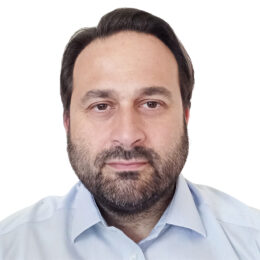
Antonio Castelo, PhD
Technology Expert for Bio-Medical and Lasers
Event Manager
Logistics, venue, accommodation, and transportation

Useful resources
Related
Market Reports
Market Reports


2026


Related
Upcoming Events
Upcoming Events


OnLine

26 October 2026.
Online Event
OnLine

28 October 2026.
Online Event
OnSite

4-5 November 2026.
Bordeaux, France
OnSite

9 November 2026.
Regensburg, Germany
OnLine

9 November 2026.
Online Event

Related
Past Events
OnLine

19 October 2026.
Online Event
Registration Closed
OnSite

13-14 October 2026.
Milan, Italy
Registration Closed
OnLine

12 October 2026.
Online Event
Registration Closed
