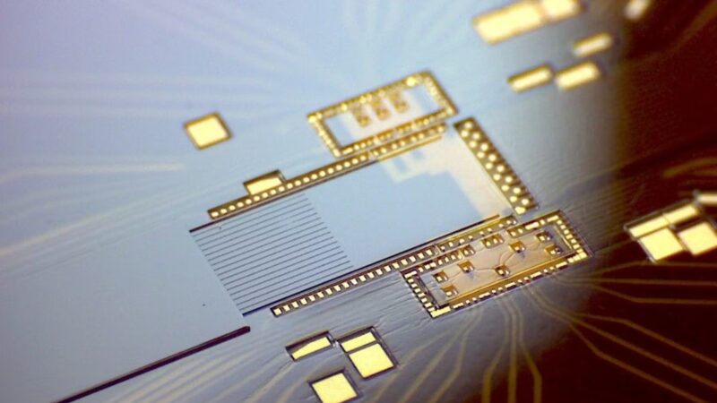
The field of photonic integrated circuits (PICs) has experienced remarkable growth in recent years, enabling a wide range of applications such as high-speed data communications, advanced sensing technologies, and LiDAR systems. But to fully unlock the potential of integrated photonics, efficient and innovative packaging solutions are essential.
Packaging covers a range of techniques and technical competencies to improve signal and power distribution, enhance optical performance, manage thermal effects, and provide mechanical, electrical, and environmental protection to the devices while at the same time enabling their connection to the outside world. It encompasses processes like die bonding, polishing, active alignment, hermetic sealing, and more.
Ivan Nikitski, features in this article published at Laser Focus World, European companies that are at the forefront of developing groundbreaking approaches to the packaging of PICs like PIXAPP Pilot Line , PHIX Photonics Assembly, ICON Photonics, AT&S, vario-optics ag, Nanoscribe, ficonTEC and Yelo.

